-
Products
- Application
- Company
-
Services
- Resources
- News
-
Contact Us

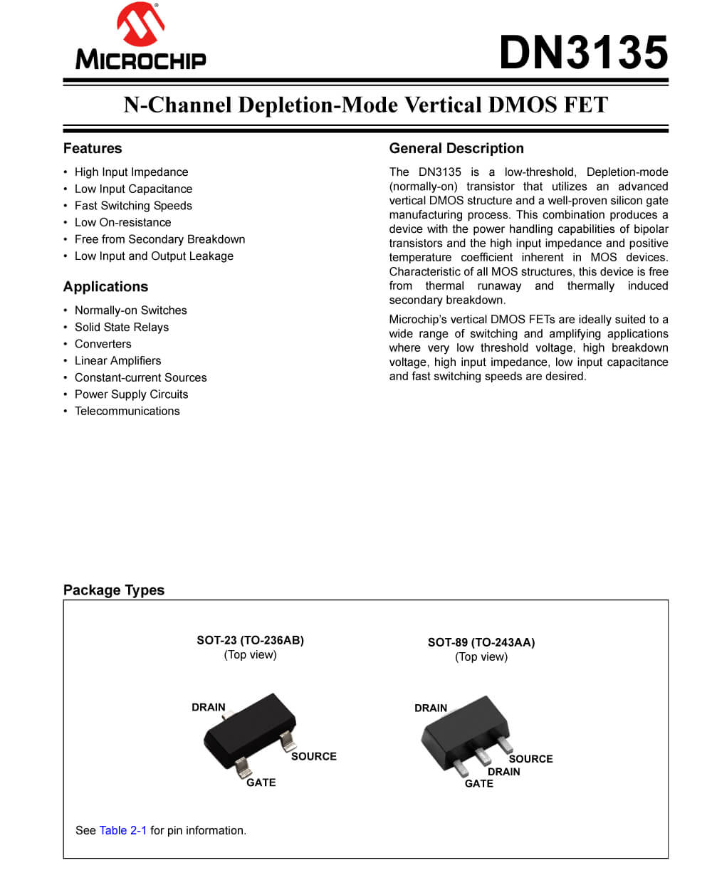
High Input Impedance
Low Input Capacitance
Fast Switching Speeds
Low On-resistance
Free from Secondary Breakdown
Low Input and Output Leakage
| ECCN (US) | EAR99 |
| Part Status | Active |
| HTS | 8541290095 |
| Automotive | No |
| PPAP | No |
| Product Category | Power MOSFET |
| Material | Si |
| Configuration | Single Dual Drain |
| Process Technology | VDMOS |
| Channel Mode | Depletion |
| Channel Type | N |
| Number of Elements per Chip | 1 |
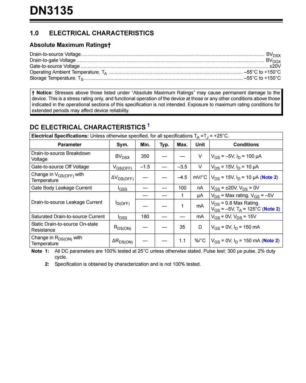
| Maximum Drain Source Voltage (V) | 350 |
| Maximum Gate Source Voltage (V) | 卤20 |
| Maximum Continuous Drain Current (A) | 0.135 |
| Maximum Gate Source Leakage Current (nA) | 100 |
| Maximum IDSS (uA) | 180000 (Min) |
| Maximum Drain Source Resistance (mOhm) | 35000@0V |
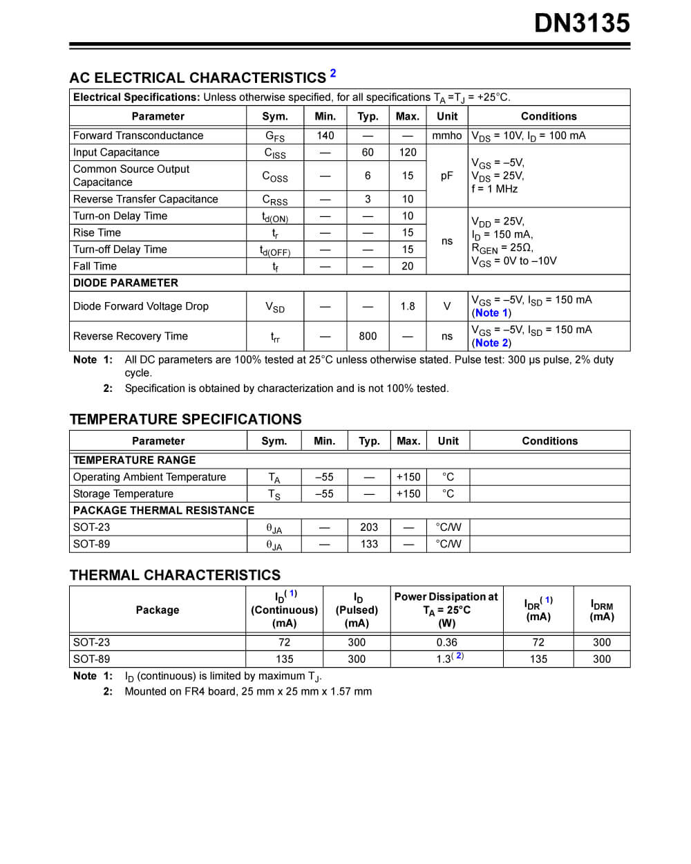
| Typical Input Capacitance @ Vds (pF) | 60@25V |
| Typical Reverse Transfer Capacitance @ Vds (pF) | 3@25V |
| Typical Output Capacitance (pF) | 6 |
| Maximum Power Dissipation (mW) | 1300 |
| Typical Fall Time (ns) | 20 (Max) |
| Typical Rise Time (ns) | 15 (Max) |
| Typical Turn-Off Delay Time (ns) | 15 (Max) |
| Typical Turn-On Delay Time (ns) | 10 (Max) |
| Minimum Operating Temperature (C) | -55 |
| Maximum Operating Temperature (C) | 150 |
| Packaging | Tape and Reel |
| Maximum Positive Gate Source Voltage (V) | 20 |
| Maximum Power Dissipation on PCB @ TC=25C (W) | 1.3 |
| Maximum Pulsed Drain Current @ TC=25C (A) | 0.3 |
| Typical Reverse Recovery Time (ns) | 800 |
| Maximum Diode Forward Voltage (V) | 1.8 |
| Mounting | Surface Mount |
| Package Height | 1.6 (Max) |
| Package Width | 2.6 (Max) |
| Package Length | 4.6 (Max) |
| PCB changed | 3 |
| Tab | Tab |
| Supplier Package | SOT-89 |
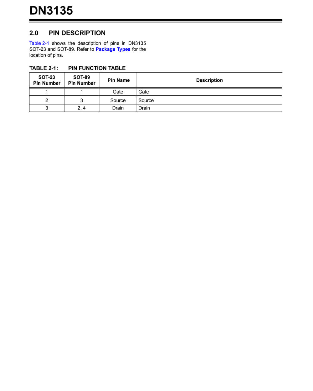
| Pin Count | 4 |


